Digital functional test systems have been part of the test landscape for over 40 years. The earliest test systems employed simple, static digital test capabilities. However, as the performance and complexity of these digital devices, modules, and systems evolved, the digital test instrumentation advanced as well. In particular, the on-going advancements associated with device toggle rates have placed a corresponding demand for ever-higher performance on the test instrumentation and systems, with today’s high-end semiconductor test systems offering multi-GHz test capabilities with attendant high power dissipation.
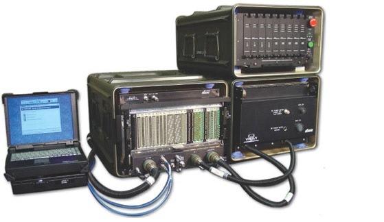
For military-aerospace applications, digital functional test has always presented a unique set of requirements and challenges. Unlike the test requirements associated with high-end device test, M-A applications are primarily focused on supporting module and system level test. Consequently, “bleeding edge” digital test performance is not required; however, a broad range of test flexibility and capability is required. The test systems and associated digital subsystems are tasked with supporting a broad portfolio of both legacy and current generation electronic assemblies, since these test systems are being used to service products in the field as well as test new generation products in the factory. More specifically, test systems deployed in the field (such as the VIPER/T shown in Figure 1) have the added constraints of both size and power dissipation – with the requirement that these systems be portable and exhibit high reliability.
 Figure 1: VIPER/T Test System Figure 1: VIPER/T Test System
The digital subsystem’s capabilities associated with these types of systems include:
- Support vector rates of at least 50 MHz with timing per pin, multiple time sets and a flexible sequencer.
- Offer a compact footprint and modular architecture, supporting up to 512 channels within a single chassis.
- Offer a wide programmable drive / sense voltage range, which allows support for both legacy applications as well as current technologies.
- Flexible architecture providing per pin programmability – maximizing flexibility for a wide range of applications.
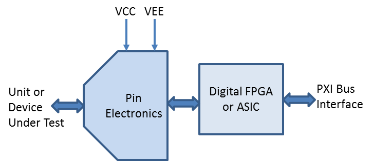
Managing the power requirements and power dissipation associated with these digital subsystems is a key requirement to achieving high reliability. Modern digital subsystems employ two major components - a high performance ASIC or FPGA which provides all of the digital logic, timing, and sequence control; and a monolithic pin electronics (PE) device(s) which interfaces to the digital logic and provides the programmable levels to the UUT or device under test (Figure 2).
 Figure 2: Digital Subsystem Architecture Figure 2: Digital Subsystem Architecture
Historically, pin electronics for digital subsystems have relied upon custom designs – some discrete, some hybrid and some full custom. However, today there are commercial vendors producing a range of pin electronic products for both semiconductor and board level test applications that offer a high level of integration and channel density. These devices are a key enabler to achieving ever higher channel densities, which also brings with it the on-going challenge of managing power dissipation and power consumption.
Today’s digital subsystems are based on open architecture, card modular platforms such as the VXI and PXI standard, with PXI being the dominant platform. And to accommodate many of the necessary features and capabilities associated with supporting M-A applications, PXI’s 6U form factor offers added PCB real estate and flexibility with regard to the use of additional power supplies, beyond the standard PXI supplies. However, power management is still a primary concern for these digital subsystems. Consider the following:
- For a wide voltage swing, high slew rate configuration, power requirements per channel can be 2.5 W or more, with a 32 channel board requiring 80 watts just for the pin electronics.
- A multi-board digital system, with all channels operating in a high voltage mode (25 V range) can require over 1200 W of power for a 512 channel system.
- Total input power for a digital subsystem can easily exceed 2 KW for a high channel count system.
As previously noted, today’s digital subsystem architectures are comprised of pin electronics and a digital ASIC or FPGA and as indicated above, the PEs are responsible for a significant portion of a digital subsystem’s power dissipation. Clearly, there is the opportunity to manage overall system power dissipation by actively managing the configuration and operating conditions associated with the PE devices.
Modern monolithic pin electronics employ two voltage rails, VH (or VCC) and VL (or VEE), which support the programmable input and output voltage levels and interface to the unit under test. These rails require a wide voltage range (-18 V to +29 V), and are the primary source of high power dissipation within the system. Consequently, by actively managing the PE devices’ operating conditions based on specific test needs, total average power and dissipation can be reduced. Incorporating programmable power supplies into the system for VL and VH and tightly controlling them by software, based on an application’s specific drive / sense levels, offers the ability to manage overall power dissipation. Under software control, active power management can be accomplished in the following ways:
- Operation with optimal rail voltages - The quiescent power dissipation for pin electronics is VL+VH times the quiescent current. However, the instrument output’s programmable levels Voh and Vol for a specific application may not be close to the VH and VL rails, with quiescent power dissipation being high regardless of the programmed Voh and Vol levels if the maximum voltages are applied to the VH and VL device rails. However, by programmatically lowering the VH and VL voltage levels such that just enough head room is required for a specific application, power dissipation can be significantly reduced. Consider the case where the programmable output level range is -10 V to +15 V. The VH voltage needs to be around 20 V and the VL voltage needs to be around -15 V to provide head room for the pin electronics circuits. If an application requires Voh=5V and Vol=0V, VH can be programmed down to 10V and VL to -5V. In this case, the pin electronics’ power dissipation will be reduced by more than 50%. By actively managing the VH and VL power supply voltages, power dissipation can be minimized, resulting in lower operating temperatures and increased reliability.
- The design of PE devices also allows for the device’s output section to be powered down without affecting the digital state of the device. This feature is extremely useful when one considers that the active duty cycle or burst time for running active digital patterns is very low. Consequently, by incorporating an “intelligent” or “smart” instrument driver that manages the digital subsystem’s power supplies, average power consumption (and power dissipation) can be reduced by over 50%.
- Adjustable / programmable slew rate and device bias current also provide the means to actively manage overall digital subsystem power dissipation. For those applications that require a high voltage swing, high slew rate is typically not required. Consequently, the PEs can be programmed via the instrument driver for optimum slew rate and bias levels based on specific test needs. A range of over 2 to 1 is available for managing power dissipation.
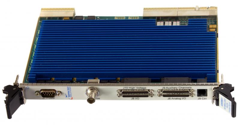
To prove out the effectiveness of the “active power” management implementation, an existing test program that employed a VXI-based digital test system was converted to execute on a 6U PXI digital subsystem (Figure 3) that employs an active power management implementation.
 Figure 3: PXI Digital Subsystem Figure 3: PXI Digital Subsystem
Compared to the legacy VXI-based digital subsystem, the PXI system demonstrated over a 50% reduction in power consumption under idle conditions - translating into lower operational costs, lower internal operating temperatures, and increased overall system reliability and up time. By leveraging the features and capabilities found in modern digital pin electronics in conjunction with use of “smart” instrument drivers, an active power management implementation can be realized that minimizes power dissipation without sacrificing system performance.
|