Beamformer integrated circuits are the key to unlocking the low latency and increased bandwidth performance promised by 5G networks, and they play a critical role in other applications areas as well including radar, imaging and remote sensing. Multiple beamforming devices are integrated into an RF front end as part of the antenna assembly, which is then programmed to form the desired overall radiation pattern. Importantly, the ability to steer the RF signal by shifting the phase of the output is essential for accurate and repeatable signal transmission and reception.
Test engineers face a new set of challenges as they transition these devices from the laboratory to a high-volume production environment.
Increased operating frequencies ranging from 44 GHz to 53 GHz impact virtually every aspect of the test system design and implementation, necessitating a fresh look at traditional approaches. |
|
Marvin Test Solutions’ GENASYS Semi Series 5G mmWave semiconductor production test systems meet and exceed the requirements of testing these devices with laboratory performance at the speeds required by OSAT (Outsourced Semiconductor Assembly and Test) production.
GENASYS Semi is the most advanced open-architecture semiconductor test platform in the industry, delivering exceptional system features and capabilities that were once only found in proprietary “big iron” ATE systems. The compact, flexible design can be configured as a benchtop system, or with an integrated manipulator, without impacting speed, measurement performance or up-time.
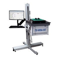
GENASYS Semi TS-900e-5G Series is the industry’s first production 5G / mmWave semiconductor solution capable of testing 40 GHz to 53 GHz devices, supporting up to 20 independent 53 GHz channels. Laboratory grade PXIe RF instrumentation is coupled with a high-performance receiver interface to deliver the most accurate and repeatable production VNA / S-parameter test performance in the industry. PXIe or LXI RF instrumentation options are available, with the ability to expand VNA channel capacity as needed, making this the ideal solution for packaged or wafer test / characterization of mmWave devices. |  |
The innovative test interface delivers proven high-performance connectivity to the device under test (DUT), with field configurable receiver interface pin blocks that allow users to upgrade the receiver as test needs change or new application requirements emerge. Furthermore, GENASYS Semi solutions are compatible with industry standard probe stations, device handlers (Opus 3, TEL, Seiko Epson E8040/ E8080), and manipulators (Reid-Ashman OM-1069, inTest).
ATEasy® Test Executive and Integrated Development Environment provides a full suite of digital and parametric test capabilities, allowing users to quickly develop and easily maintain test applications including a SPI/I2C interface for controlling and monitoring the DUT.
Want to know more?
For more details about how GENASYS Semi is redefining 5G mmWave semiconductor device test, view our recorded webinar online here.
Or contact us today to discuss your requirements and learn how We Make Test Easy™ for semiconductor device manufacturers. |